Quantum
-
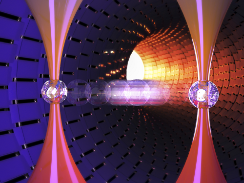 Using light to throw and catch atoms to open up a new chapter for quantum computing
The technology to move and arrange atoms, the most basic component of a quantum computer, is very important to Rydberg quantum computing research. However, to place the atoms at the desired location, the atoms must be captured and transported one by one using a highly focused laser beam, commonly referred to as an optical tweezer. and, the quantum information of the atoms is likely to change midway.
KAIST (President Kwang Hyung Lee) announced on the 27th that a research team led by Professor Jaewook Ahn of the Department of Physics developed a technology to throw and receive rubidium atoms one by one using a laser beam.
The research team developed a method to throw and receive atoms which would minimize the time the optical tweezers are in contact with the atoms in which the quantum information the atoms carry may change. The research team used the characteristic that the rubidium atoms, which are kept at a very low temperature of 40μK below absolute zero, move very sensitively to the electromagnetic force applied by light along the focal point of the light tweezers.
The research team accelerated the laser of an optical tweezer to give an optical kick to an atom to send it to a target, then caught the flying atom with another optical tweezer to stop it. The atom flew at a speed of 65 cm/s, and traveled up to 4.2 μm. Compared to the existing technique of guiding the atoms with the optical tweezers, the technique of throwing and receiving atoms eliminates the need to calculate the transporting path for the tweezers, and makes it easier to fix the defects in the atomic arrangement. As a result, it is effective in generating and maintaining a large number of atomic arrangements, and when the technology is used to throw and receive flying atom qubits, it will be used in studying new and more powerful quantum computing methods that presupposes the structural changes in quantum arrangements.
"This technology will be used to develop larger and more powerful Rydberg quantum computers," says Professor Jaewook Ahn. “In a Rydberg quantum computer,” he continues, “atoms are arranged to store quantum information and interact with neighboring atoms through electromagnetic forces to perform quantum computing. The method of throwing an atom away for quick reconstruction the quantum array can be an effective way to fix an error in a quantum computer that requires a removal or replacement of an atom.”
The research, which was conducted by doctoral students Hansub Hwang and Andrew Byun of the Department of Physics at KAIST and Sylvain de Léséleuc, a researcher at the National Institute of Natural Sciences in Japan, was published in the international journal, Optica, 0n March 9th. (Paper title: Optical tweezers throw and catch single atoms).
This research was carried out with the support of the Samsung Science & Technology Foundation.
<Figure 1> A schematic diagram of the atom catching and throwing technique. The optical tweezer on the left kicks the atom to throw it into a trajectory to have the tweezer on the right catch it to stop it.
2023.03.28 View 2138
Using light to throw and catch atoms to open up a new chapter for quantum computing
The technology to move and arrange atoms, the most basic component of a quantum computer, is very important to Rydberg quantum computing research. However, to place the atoms at the desired location, the atoms must be captured and transported one by one using a highly focused laser beam, commonly referred to as an optical tweezer. and, the quantum information of the atoms is likely to change midway.
KAIST (President Kwang Hyung Lee) announced on the 27th that a research team led by Professor Jaewook Ahn of the Department of Physics developed a technology to throw and receive rubidium atoms one by one using a laser beam.
The research team developed a method to throw and receive atoms which would minimize the time the optical tweezers are in contact with the atoms in which the quantum information the atoms carry may change. The research team used the characteristic that the rubidium atoms, which are kept at a very low temperature of 40μK below absolute zero, move very sensitively to the electromagnetic force applied by light along the focal point of the light tweezers.
The research team accelerated the laser of an optical tweezer to give an optical kick to an atom to send it to a target, then caught the flying atom with another optical tweezer to stop it. The atom flew at a speed of 65 cm/s, and traveled up to 4.2 μm. Compared to the existing technique of guiding the atoms with the optical tweezers, the technique of throwing and receiving atoms eliminates the need to calculate the transporting path for the tweezers, and makes it easier to fix the defects in the atomic arrangement. As a result, it is effective in generating and maintaining a large number of atomic arrangements, and when the technology is used to throw and receive flying atom qubits, it will be used in studying new and more powerful quantum computing methods that presupposes the structural changes in quantum arrangements.
"This technology will be used to develop larger and more powerful Rydberg quantum computers," says Professor Jaewook Ahn. “In a Rydberg quantum computer,” he continues, “atoms are arranged to store quantum information and interact with neighboring atoms through electromagnetic forces to perform quantum computing. The method of throwing an atom away for quick reconstruction the quantum array can be an effective way to fix an error in a quantum computer that requires a removal or replacement of an atom.”
The research, which was conducted by doctoral students Hansub Hwang and Andrew Byun of the Department of Physics at KAIST and Sylvain de Léséleuc, a researcher at the National Institute of Natural Sciences in Japan, was published in the international journal, Optica, 0n March 9th. (Paper title: Optical tweezers throw and catch single atoms).
This research was carried out with the support of the Samsung Science & Technology Foundation.
<Figure 1> A schematic diagram of the atom catching and throwing technique. The optical tweezer on the left kicks the atom to throw it into a trajectory to have the tweezer on the right catch it to stop it.
2023.03.28 View 2138 -
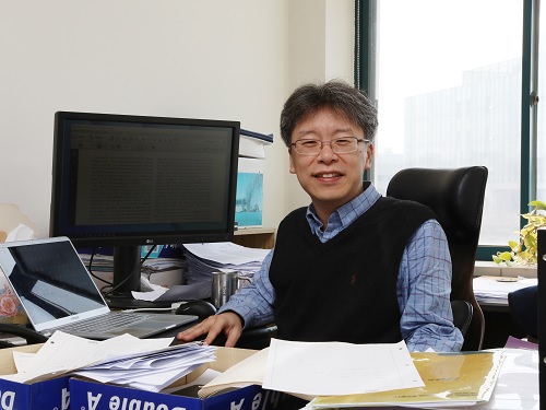
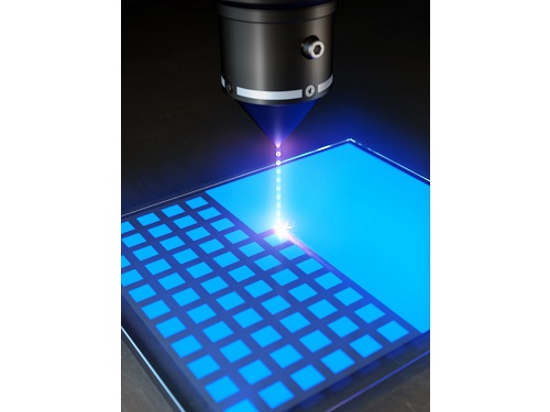 KAIST researchers develops a tech to enable production of ultrahigh-resolution LED with sub-micrometer scale pixels
Ultrahigh-resolution displays are an essential element for developing next-generation electronic products such as virtual reality (VR), augmented reality (AR), and smart watches, and can be applied not only to head-mounted displays, but also to smart glasses and smart lenses. The technology developed through this research is expected to be used to make such next-generation ultrahigh-resolution displays and other various sub-micro optoelectronic devices.
KAIST (President Kwang Hyung Lee) announced on the 22nd that Professor Yong-Hoon Cho's research team of KAIST Department of Physics developed the core technology for an ultrahigh resolution light-emitting diode (LED) display that can realize 0.5 micron-scale pixels smaller than 1/100 of the average hair thickness (about 100 microns) using focused ion beams.
Commonly, pixelation of ultrahigh-resolution LED displays usually relies on the etching method that physically cuts the area around the pixel, but as the pixel becomes smaller due to the occurrence of various defects around it, leading to side-effects of having leakage of current increased and light-emission efficiency decreased. In addition, various complex processes such as patterning for pixelation and post-processing for prevention of leakage current are required.
Professor Yong-Hoon Cho's research team developed a technology that can create pixels down to the size of a microscale without the complicated pre- and post-processing using a focused ion beam. This method has the advantage of being able to freely set the shape of the emitting pixel without causing any structural deformation on the material surface by controlling the intensity of the focused ion beam.
The focused ion beam technology has been widely used for ultrahigh-magnification imaging and nanostructure fabrication in fields such as materials engineering and biology. However, when a focused ion beam is used on a light emitting body such as an LED, light emission of a portion hit by the beam and a surrounding area rapidly decreases, which has been a barrier to fabricating a nano-scale light emitting structure. Upon facing this issue, Professor Cho's research team began the research on the idea that if they turned things around to use these problematic phenomena, they can be used in ultra-fine pixelation method on a sub-micron scale.
The research team used a focused ion beam whose intensity was softened to the extent that the surface was not shaved, and found that not only the light-emission rapidly decreased in the area hit by the focused ion beam, but also the local resistance greatly increased. As a result, while the surface of the LED is kept flat, the portion hit by the focused ion beam is optically and electrically isolated, enabling pixelation for independent operation.
Professor Yong-Hoon Cho, who led the research, said, “We have newly developed a technology that can create sub-micron-scale pixels without complicated processes using a focused ion beam, which will be a base technology that can be applied to next-generation ultrahigh-resolution displays and nano-photoelectronic devices.”
This research in which the Master's student Ji-Hwan Moon and the Ph.D. student Baul Kim of KAIST Department of Physics participated as co-first authors, was carried out with the support of the National Research Foundation of Korea's Support Program for Mid-Career Researchers and the Institute of Information and Communications Technology Planning and Evaluation. It was published online in 'Advanced Materials' on February 13, and was also selected as the internal cover of the next offline edition. (Title: Electrically Driven Sub-Micron Light-Emitting Diode Arrays Using Maskless and Etching-Free Pixelation)
Figure 1. Schematic diagram of the technology for ultrahigh density sub-micron-sized pixels through He focused ion beam (FIB) irradiation on an LED device
Figure 2. Ultra-high-density pixelation technology of micro light-emitting diodes (μLED) through He focused ion beam (FIB) irradiation
Figure 3. Rectangular pixels of different sizes (surface structure picture and luminescence picture) realized by a focused ion beam. Luminescence pictures of pixel arrays ranging in size from 20 µm x 20 µm to 0.5 µm x 0.5 µm, with surface flatness maintained.
2023.03.08 View 2483
KAIST researchers develops a tech to enable production of ultrahigh-resolution LED with sub-micrometer scale pixels
Ultrahigh-resolution displays are an essential element for developing next-generation electronic products such as virtual reality (VR), augmented reality (AR), and smart watches, and can be applied not only to head-mounted displays, but also to smart glasses and smart lenses. The technology developed through this research is expected to be used to make such next-generation ultrahigh-resolution displays and other various sub-micro optoelectronic devices.
KAIST (President Kwang Hyung Lee) announced on the 22nd that Professor Yong-Hoon Cho's research team of KAIST Department of Physics developed the core technology for an ultrahigh resolution light-emitting diode (LED) display that can realize 0.5 micron-scale pixels smaller than 1/100 of the average hair thickness (about 100 microns) using focused ion beams.
Commonly, pixelation of ultrahigh-resolution LED displays usually relies on the etching method that physically cuts the area around the pixel, but as the pixel becomes smaller due to the occurrence of various defects around it, leading to side-effects of having leakage of current increased and light-emission efficiency decreased. In addition, various complex processes such as patterning for pixelation and post-processing for prevention of leakage current are required.
Professor Yong-Hoon Cho's research team developed a technology that can create pixels down to the size of a microscale without the complicated pre- and post-processing using a focused ion beam. This method has the advantage of being able to freely set the shape of the emitting pixel without causing any structural deformation on the material surface by controlling the intensity of the focused ion beam.
The focused ion beam technology has been widely used for ultrahigh-magnification imaging and nanostructure fabrication in fields such as materials engineering and biology. However, when a focused ion beam is used on a light emitting body such as an LED, light emission of a portion hit by the beam and a surrounding area rapidly decreases, which has been a barrier to fabricating a nano-scale light emitting structure. Upon facing this issue, Professor Cho's research team began the research on the idea that if they turned things around to use these problematic phenomena, they can be used in ultra-fine pixelation method on a sub-micron scale.
The research team used a focused ion beam whose intensity was softened to the extent that the surface was not shaved, and found that not only the light-emission rapidly decreased in the area hit by the focused ion beam, but also the local resistance greatly increased. As a result, while the surface of the LED is kept flat, the portion hit by the focused ion beam is optically and electrically isolated, enabling pixelation for independent operation.
Professor Yong-Hoon Cho, who led the research, said, “We have newly developed a technology that can create sub-micron-scale pixels without complicated processes using a focused ion beam, which will be a base technology that can be applied to next-generation ultrahigh-resolution displays and nano-photoelectronic devices.”
This research in which the Master's student Ji-Hwan Moon and the Ph.D. student Baul Kim of KAIST Department of Physics participated as co-first authors, was carried out with the support of the National Research Foundation of Korea's Support Program for Mid-Career Researchers and the Institute of Information and Communications Technology Planning and Evaluation. It was published online in 'Advanced Materials' on February 13, and was also selected as the internal cover of the next offline edition. (Title: Electrically Driven Sub-Micron Light-Emitting Diode Arrays Using Maskless and Etching-Free Pixelation)
Figure 1. Schematic diagram of the technology for ultrahigh density sub-micron-sized pixels through He focused ion beam (FIB) irradiation on an LED device
Figure 2. Ultra-high-density pixelation technology of micro light-emitting diodes (μLED) through He focused ion beam (FIB) irradiation
Figure 3. Rectangular pixels of different sizes (surface structure picture and luminescence picture) realized by a focused ion beam. Luminescence pictures of pixel arrays ranging in size from 20 µm x 20 µm to 0.5 µm x 0.5 µm, with surface flatness maintained.
2023.03.08 View 2483 -
 Professor June-Koo Rhee’s Team Wins the QHack Open Hackathon Science Challenge
The research team consisting of three master students Ju-Young Ryu, Jeung-rak Lee, and Eyel Elala in Professor June-Koo Rhee’s group from the KAIST IRTC of Quantum Computing for AI has won the first place at the QHack 2022 Open Hackathon Science Challenge.
The QHack 2022 Open Hackathon is one of the world’s prestigious quantum software hackathon events held by US Xanadu, in which 250 people from 100 countries participate. Major sponsors such as IBM Quantum, AWS, CERN QTI, and Google Quantum AI proposed challenging problems, and a winning team is selected judged on team projects in each of the 13 challenges.
The KAIST team supervised by Professor Rhee received the First Place prize on the Science Challenge which was organized by the CERN QTI of the European Communities. The team will be awarded an opportunity to tour CERN’s research lab in Europe for one week along with an online internship.
The students on the team presented a method for “Leaning Based Error Mitigation for VQE,” in which they implemented an LBEM protocol to lower the error in quantum computing, and leveraged the protocol in the VQU algorithm which is used to calculate the ground state energy of a given molecule.
Their research successfully demonstrated the ability to effectively mitigate the error in IBM Quantum hardware and the virtual error model. In conjunction, Professor June-Koo (Kevin) Rhee founded a quantum computing venture start-up, Qunova Computing(https://qunovacomputing.com), with technology tranfer from the KAIST ITRC of Quantum Computing for AI. Qunova Computing is one of the frontier of the quantum software industry in Korea.
2022.04.08 View 3347
Professor June-Koo Rhee’s Team Wins the QHack Open Hackathon Science Challenge
The research team consisting of three master students Ju-Young Ryu, Jeung-rak Lee, and Eyel Elala in Professor June-Koo Rhee’s group from the KAIST IRTC of Quantum Computing for AI has won the first place at the QHack 2022 Open Hackathon Science Challenge.
The QHack 2022 Open Hackathon is one of the world’s prestigious quantum software hackathon events held by US Xanadu, in which 250 people from 100 countries participate. Major sponsors such as IBM Quantum, AWS, CERN QTI, and Google Quantum AI proposed challenging problems, and a winning team is selected judged on team projects in each of the 13 challenges.
The KAIST team supervised by Professor Rhee received the First Place prize on the Science Challenge which was organized by the CERN QTI of the European Communities. The team will be awarded an opportunity to tour CERN’s research lab in Europe for one week along with an online internship.
The students on the team presented a method for “Leaning Based Error Mitigation for VQE,” in which they implemented an LBEM protocol to lower the error in quantum computing, and leveraged the protocol in the VQU algorithm which is used to calculate the ground state energy of a given molecule.
Their research successfully demonstrated the ability to effectively mitigate the error in IBM Quantum hardware and the virtual error model. In conjunction, Professor June-Koo (Kevin) Rhee founded a quantum computing venture start-up, Qunova Computing(https://qunovacomputing.com), with technology tranfer from the KAIST ITRC of Quantum Computing for AI. Qunova Computing is one of the frontier of the quantum software industry in Korea.
2022.04.08 View 3347 -
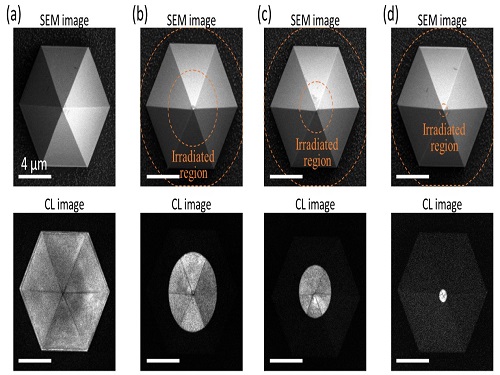 Quantum Emitters: Beyond Crystal Clear to Single-Photon Pure
‘Nanoscale Focus Pinspot’ can quench only the background noise without changing the optical properties of the quantum emitter and the built-in photonic structure
Photons, fundamental particles of light, are carrying these words to your eyes via the light from your computer screen or phone. Photons play a key role in the next-generation quantum information technology, such as quantum computing and communications. A quantum emitter, capable of producing a single, pure photon, is the crux of such technology but has many issues that have yet to be solved, according to KAIST researchers.
A research team under Professor Yong-Hoon Cho has developed a technique that can isolate the desired quality emitter by reducing the noise surrounding the target with what they have dubbed a ‘nanoscale focus pinspot.’ They published their results on June 24 in ACS Nano.
“The nanoscale focus pinspot is a structurally nondestructive technique under an extremely low dose ion beam and is generally applicable for various platforms to improve their single-photon purity while retaining the integrated photonic structures,” said lead author Yong-Hoon Cho from the Department of Physics at KAIST.
To produce single photons from solid state materials, the researchers used wide-bandgap semiconductor quantum dots — fabricated nanoparticles with specialized potential properties, such as the ability to directly inject current into a small chip and to operate at room temperature for practical applications. By making a quantum dot in a photonic structure that propagates light, and then irradiating it with helium ions, researchers theorized that they could develop a quantum emitter that could reduce the unwanted noisy background and produce a single, pure photon on demand.
Professor Cho explained, “Despite its high resolution and versatility, a focused ion beam typically suppresses the optical properties around the bombarded area due to the accelerated ion beam’s high momentum. We focused on the fact that, if the focused ion beam is well controlled, only the background noise can be selectively quenched with high spatial resolution without destroying the structure.”
In other words, the researchers focused the ion beam on a mere pin prick, effectively cutting off the interactions around the quantum dot and removing the physical properties that could negatively interact with and degrade the photon purity emitted from the quantum dot.
“It is the first developed technique that can quench the background noise without changing the optical properties of the quantum emitter and the built-in photonic structure,” Professor Cho asserted.
Professor Cho compared it to stimulated emission depletion microscopy, a technique used to decrease the light around the area of focus, but leaving the focal point illuminated. The result is increased resolution of the desired visual target.
“By adjusting the focused ion beam-irradiated region, we can select the target emitter with nanoscale resolution by quenching the surrounding emitter,” Professor Cho said. “This nanoscale selective-quenching technique can be applied to various material and structural platforms and further extended for applications such as optical memory and high-resolution micro displays.” Korea’s National Research Foundation and the Samsung Science and Technology Foundation supported this work.
-PublicationMinho Choi, Seongmoon Jun, and Yong-Hoon Cho et al. ACS Nano‘Nanoscale Focus Pinspot for High-Purity Quantum Emitters via Focused-Ion-Beam-Induced Luminescence Quenching,’(https://pubs.acs.org/doi/10.1021/acsnano.1c00587)
-ProfileProfessor Yong-Hoon ChoQuantum & Nanobio Photonics Laboratoryhttp://qnp.kaist.ac.kr/
Department of PhysicsKAIST
2021.09.02 View 5897
Quantum Emitters: Beyond Crystal Clear to Single-Photon Pure
‘Nanoscale Focus Pinspot’ can quench only the background noise without changing the optical properties of the quantum emitter and the built-in photonic structure
Photons, fundamental particles of light, are carrying these words to your eyes via the light from your computer screen or phone. Photons play a key role in the next-generation quantum information technology, such as quantum computing and communications. A quantum emitter, capable of producing a single, pure photon, is the crux of such technology but has many issues that have yet to be solved, according to KAIST researchers.
A research team under Professor Yong-Hoon Cho has developed a technique that can isolate the desired quality emitter by reducing the noise surrounding the target with what they have dubbed a ‘nanoscale focus pinspot.’ They published their results on June 24 in ACS Nano.
“The nanoscale focus pinspot is a structurally nondestructive technique under an extremely low dose ion beam and is generally applicable for various platforms to improve their single-photon purity while retaining the integrated photonic structures,” said lead author Yong-Hoon Cho from the Department of Physics at KAIST.
To produce single photons from solid state materials, the researchers used wide-bandgap semiconductor quantum dots — fabricated nanoparticles with specialized potential properties, such as the ability to directly inject current into a small chip and to operate at room temperature for practical applications. By making a quantum dot in a photonic structure that propagates light, and then irradiating it with helium ions, researchers theorized that they could develop a quantum emitter that could reduce the unwanted noisy background and produce a single, pure photon on demand.
Professor Cho explained, “Despite its high resolution and versatility, a focused ion beam typically suppresses the optical properties around the bombarded area due to the accelerated ion beam’s high momentum. We focused on the fact that, if the focused ion beam is well controlled, only the background noise can be selectively quenched with high spatial resolution without destroying the structure.”
In other words, the researchers focused the ion beam on a mere pin prick, effectively cutting off the interactions around the quantum dot and removing the physical properties that could negatively interact with and degrade the photon purity emitted from the quantum dot.
“It is the first developed technique that can quench the background noise without changing the optical properties of the quantum emitter and the built-in photonic structure,” Professor Cho asserted.
Professor Cho compared it to stimulated emission depletion microscopy, a technique used to decrease the light around the area of focus, but leaving the focal point illuminated. The result is increased resolution of the desired visual target.
“By adjusting the focused ion beam-irradiated region, we can select the target emitter with nanoscale resolution by quenching the surrounding emitter,” Professor Cho said. “This nanoscale selective-quenching technique can be applied to various material and structural platforms and further extended for applications such as optical memory and high-resolution micro displays.” Korea’s National Research Foundation and the Samsung Science and Technology Foundation supported this work.
-PublicationMinho Choi, Seongmoon Jun, and Yong-Hoon Cho et al. ACS Nano‘Nanoscale Focus Pinspot for High-Purity Quantum Emitters via Focused-Ion-Beam-Induced Luminescence Quenching,’(https://pubs.acs.org/doi/10.1021/acsnano.1c00587)
-ProfileProfessor Yong-Hoon ChoQuantum & Nanobio Photonics Laboratoryhttp://qnp.kaist.ac.kr/
Department of PhysicsKAIST
2021.09.02 View 5897 -
 Professor Heung-Sun Sim the MSIT Scientist of July
Professor Heung-Sun Sim from the Department of Physics was selected as the Scientist of July by the Ministry of Science and ICT. Professor Sim was recognized for his research of the Kondo effect, which opened a novel way to engineer spin screening and entanglement by directly observing a quantum phenomenon known as a Kondo screening cloud. His research revealed that the cloud can mediate interactions between distant spins confined in quantum dots, which is a necessary protocol for semiconductor spin-based quantum information processing. This phenomenon is essentially a cloud that masks magnetic impurities in a material. It was known to exist but its spatial extension had never been observed, creating controversy over whether such an extension actually existed. The research was reported in Nature in March 2020. With this award, Professor Sim received 10 million KRW in prize money.
2021.07.12 View 4482
Professor Heung-Sun Sim the MSIT Scientist of July
Professor Heung-Sun Sim from the Department of Physics was selected as the Scientist of July by the Ministry of Science and ICT. Professor Sim was recognized for his research of the Kondo effect, which opened a novel way to engineer spin screening and entanglement by directly observing a quantum phenomenon known as a Kondo screening cloud. His research revealed that the cloud can mediate interactions between distant spins confined in quantum dots, which is a necessary protocol for semiconductor spin-based quantum information processing. This phenomenon is essentially a cloud that masks magnetic impurities in a material. It was known to exist but its spatial extension had never been observed, creating controversy over whether such an extension actually existed. The research was reported in Nature in March 2020. With this award, Professor Sim received 10 million KRW in prize money.
2021.07.12 View 4482 -
 Quantum Laser Turns Energy Loss into Gain
A new laser that generates quantum particles can recycle lost energy for highly efficient, low threshold laser applications
Scientists at KAIST have fabricated a laser system that generates highly interactive quantum particles at room temperature. Their findings, published in the journal Nature Photonics, could lead to a single microcavity laser system that requires lower threshold energy as its energy loss increases.
The system, developed by KAIST physicist Yong-Hoon Cho and colleagues, involves shining light through a single hexagonal-shaped microcavity treated with a loss-modulated silicon nitride substrate. The system design leads to the generation of a polariton laser at room temperature, which is exciting because this usually requires cryogenic temperatures.
The researchers found another unique and counter-intuitive feature of this design. Normally, energy is lost during laser operation. But in this system, as energy loss increased, the amount of energy needed to induce lasing decreased. Exploiting this phenomenon could lead to the development of high efficiency, low threshold lasers for future quantum optical devices.
“This system applies a concept of quantum physics known as parity-time reversal symmetry,” explains Professor Cho. “This is an important platform that allows energy loss to be used as gain. It can be used to reduce laser threshold energy for classical optical devices and sensors, as well as quantum devices and controlling the direction of light.”
The key is the design and materials. The hexagonal microcavity divides light particles into two different modes: one that passes through the upward-facing triangle of the hexagon and another that passes through its downward-facing triangle. Both modes of light particles have the same energy and path but don’t interact with each other.
However, the light particles do interact with other particles called excitons, provided by the hexagonal microcavity, which is made of semiconductors. This interaction leads to the generation of new quantum particles called polaritons that then interact with each other to generate the polariton laser. By controlling the degree of loss between the microcavity and the semiconductor substrate, an intriguing phenomenon arises, with the threshold energy becoming smaller as energy loss increases. This research was supported by the Samsung Science and Technology Foundation and Korea’s National Research Foundation.
-PublicationSong,H.G, Choi, M, Woo, K.Y. Yong-Hoon Cho Room-temperature polaritonic non-Hermitian system with single microcavityNature Photonics (https://doi.org/10.1038/s41566-021-00820-z)
-ProfileProfessor Yong-Hoon ChoQuantum & Nanobio Photonics Laboratoryhttp://qnp.kaist.ac.kr/
Department of PhysicsKAIST
2021.07.07 View 6034
Quantum Laser Turns Energy Loss into Gain
A new laser that generates quantum particles can recycle lost energy for highly efficient, low threshold laser applications
Scientists at KAIST have fabricated a laser system that generates highly interactive quantum particles at room temperature. Their findings, published in the journal Nature Photonics, could lead to a single microcavity laser system that requires lower threshold energy as its energy loss increases.
The system, developed by KAIST physicist Yong-Hoon Cho and colleagues, involves shining light through a single hexagonal-shaped microcavity treated with a loss-modulated silicon nitride substrate. The system design leads to the generation of a polariton laser at room temperature, which is exciting because this usually requires cryogenic temperatures.
The researchers found another unique and counter-intuitive feature of this design. Normally, energy is lost during laser operation. But in this system, as energy loss increased, the amount of energy needed to induce lasing decreased. Exploiting this phenomenon could lead to the development of high efficiency, low threshold lasers for future quantum optical devices.
“This system applies a concept of quantum physics known as parity-time reversal symmetry,” explains Professor Cho. “This is an important platform that allows energy loss to be used as gain. It can be used to reduce laser threshold energy for classical optical devices and sensors, as well as quantum devices and controlling the direction of light.”
The key is the design and materials. The hexagonal microcavity divides light particles into two different modes: one that passes through the upward-facing triangle of the hexagon and another that passes through its downward-facing triangle. Both modes of light particles have the same energy and path but don’t interact with each other.
However, the light particles do interact with other particles called excitons, provided by the hexagonal microcavity, which is made of semiconductors. This interaction leads to the generation of new quantum particles called polaritons that then interact with each other to generate the polariton laser. By controlling the degree of loss between the microcavity and the semiconductor substrate, an intriguing phenomenon arises, with the threshold energy becoming smaller as energy loss increases. This research was supported by the Samsung Science and Technology Foundation and Korea’s National Research Foundation.
-PublicationSong,H.G, Choi, M, Woo, K.Y. Yong-Hoon Cho Room-temperature polaritonic non-Hermitian system with single microcavityNature Photonics (https://doi.org/10.1038/s41566-021-00820-z)
-ProfileProfessor Yong-Hoon ChoQuantum & Nanobio Photonics Laboratoryhttp://qnp.kaist.ac.kr/
Department of PhysicsKAIST
2021.07.07 View 6034 -
 KAIST Joins IBM Q Network to Accelerate Quantum Computing Research and Foster Quantum Industry
KAIST has joined the IBM Q Network, a community of Fortune 500 companies, academic institutions, startups, and research labs working with IBM to advance quantum computing for business and science.
As the IBM Q Network’s first academic partner in Korea, KAIST will use IBM's advanced quantum computing systems to carry out research projects that advance quantum information science and explore early applications. KAIST will also utilize IBM Quantum resources for talent training and education in preparation for building a quantum workforce for the quantum computing era that will bring huge changes to science and business. By joining the network, KAIST will take a leading role in fostering the ecosystem of quantum computing in Korea, which is expected to be a necessary enabler to realize the Fourth Industrial Revolution.
Professor June-Koo Rhee who also serves as Director of the KAIST Information Technology Research Center (ITRC) of Quantum Computing for AI has led the agreement on KAIST’s joining the IBM Q Network. Director Rhee described quantum computing as "a new technology that can calculate mathematical challenges at very high speed and low power” and also as “one that will change the future.”
Director Rhee said, “Korea started investment in quantum computing relatively late, and thus requires to take bold steps with innovative R&D strategies to pave the roadmap for the next technological leap in the field”. With KAIST joining the IBM Q Network, “Korea will be better equipped to establish a quantum industry, an important foundation for securing national competitiveness,” he added.
The KAIST ITRC of Quantum Computing for AI has been using the publicly available IBM Quantum Experience delivered over the IBM Cloud for research, development and training of quantum algorithms such as quantum artificial intelligence, quantum chemical calculation, and quantum computing education.
KAIST will have access to the most advanced IBM Quantum systems to explore practical research and experiments such as diagnosis of diseases based on quantum artificial intelligence, quantum computational chemistry, and quantum machine learning technology. In addition, knowledge exchanges and sharing with overseas universities and companies under the IBM Q Network will help KAIST strengthen the global presence of Korean technology in quantum computing.
About IBM Quantum
IBM Quantum is an industry-first initiative to build quantum systems for business and science applications. For more information about IBM's quantum computing efforts, please visit www.ibm.com/ibmq.
For more information about the IBM Q Network, as well as a full list of all partners, members, and hubs, visit https://www.research.ibm.com/ibm-q/network/
©Thumbnail Image: IBM.
(END)
2020.09.29 View 6084
KAIST Joins IBM Q Network to Accelerate Quantum Computing Research and Foster Quantum Industry
KAIST has joined the IBM Q Network, a community of Fortune 500 companies, academic institutions, startups, and research labs working with IBM to advance quantum computing for business and science.
As the IBM Q Network’s first academic partner in Korea, KAIST will use IBM's advanced quantum computing systems to carry out research projects that advance quantum information science and explore early applications. KAIST will also utilize IBM Quantum resources for talent training and education in preparation for building a quantum workforce for the quantum computing era that will bring huge changes to science and business. By joining the network, KAIST will take a leading role in fostering the ecosystem of quantum computing in Korea, which is expected to be a necessary enabler to realize the Fourth Industrial Revolution.
Professor June-Koo Rhee who also serves as Director of the KAIST Information Technology Research Center (ITRC) of Quantum Computing for AI has led the agreement on KAIST’s joining the IBM Q Network. Director Rhee described quantum computing as "a new technology that can calculate mathematical challenges at very high speed and low power” and also as “one that will change the future.”
Director Rhee said, “Korea started investment in quantum computing relatively late, and thus requires to take bold steps with innovative R&D strategies to pave the roadmap for the next technological leap in the field”. With KAIST joining the IBM Q Network, “Korea will be better equipped to establish a quantum industry, an important foundation for securing national competitiveness,” he added.
The KAIST ITRC of Quantum Computing for AI has been using the publicly available IBM Quantum Experience delivered over the IBM Cloud for research, development and training of quantum algorithms such as quantum artificial intelligence, quantum chemical calculation, and quantum computing education.
KAIST will have access to the most advanced IBM Quantum systems to explore practical research and experiments such as diagnosis of diseases based on quantum artificial intelligence, quantum computational chemistry, and quantum machine learning technology. In addition, knowledge exchanges and sharing with overseas universities and companies under the IBM Q Network will help KAIST strengthen the global presence of Korean technology in quantum computing.
About IBM Quantum
IBM Quantum is an industry-first initiative to build quantum systems for business and science applications. For more information about IBM's quantum computing efforts, please visit www.ibm.com/ibmq.
For more information about the IBM Q Network, as well as a full list of all partners, members, and hubs, visit https://www.research.ibm.com/ibm-q/network/
©Thumbnail Image: IBM.
(END)
2020.09.29 View 6084 -
 Highly Efficient Charge-to-Spin Interconversion in Graphene Heterostructures
Researchers present a new route for designing a graphene-based active spintronic component
KAIST physicists described a route to design the energy-efficient generation, manipulation and detection of spin currents using nonmagnetic two-dimensional materials. The research team, led by Professor Sungjae Cho, observed highly efficient charge-to-spin interconversion via the gate-tunable Rashba-Edelstien effect (REE) in graphene heterostructures.
This research paves the way for the application of graphene as an active spintronic component for generating, controlling, and detecting spin current without ferromagnetic electrodes or magnetic fields.
Graphene is a promising spintronic component owing to its long spin diffusion length. However, its small spin-orbit coupling limits the potential of graphene in spintronic applications since graphene cannot be used to generate, control, or detect spin current.
“We successfully increased the spin-orbit coupling of graphene by stacking graphene on top of 2H-TaS2, which is one of the transition metal dichalcogenide materials with the largest spin-orbit coupling. Graphene now can be used to generate, control, and detect spin current,” Professor Cho said.
The Rashba-Edelstein effect is a physical mechanism that enables charge current-to-spin current interconversion by spin-dependent band structure induced by the Rashba effect, a momentum-dependent splitting of spin bands in low-dimensional condensed matter systems.
Professor Cho’s group demonstrated the gate-tunable Rashba-Edelstein effect in a multilayer graphene for the first time. The Rahsba-Edelstein effect allows the two-dimensional conduction electrons of graphene to be magnetized by an applied charge current and form a spin current. Furthermore, as the Fermi level of graphene, tuned by gate voltage, moves from the valence to conduction band, the spin current generated by graphene reversed its spin direction.
This spin reversal is useful in the design of low-power-consumption transistors utilizing spins in that it provides the carrier “On” state with spin up holes (or spin down electrons) and the "Off" state with zero net spin polarization at so called “charge neutrality point” where numbers of electrons and holes are equal.
“Our work is the first demonstration of charge-to-spin interconversion in a metallic TMD (transition-metal dichalcogenides) and graphene heterostructure with a spin polarization state controlled by a gate. We expect that the all-electrical spin-switching effect and the reversal of non-equilibrium spin polarization by the application of gate voltage is applicable for the energy-efficient generation and manipulation of spin currents using nonmagnetic van der Waals materials,” explained Professor Cho.
This study (https://pubs.acs.org/doi/10.1021/acsnano.0c01037) was supported by the National Research Foundation of Korea.
Publication:
Lijun Li, Jin Zhang, Gyuho Myeong, Wongil Shin, Hongsik Lim, Boram Kim, Seungho Kim, Taehyeok Jin, Stuart Cavill, Beom Seo Kim, Changyoung Kim, Johannes Lischner, Aires Ferreira, and Sungjae Cho, Gate-Tunable Reversible Rashba−Edelstein Effect in a Few-Layer Graphene/2H-TaS2 Heterostructure at Room Temperature. ACS Nano 2020. Link to download the paper: https://pubs.acs.org/doi/10.1021/acsnano.0c01037
Profile:
Professor Sungjae Cho, PhD
sungjae.cho@kaist.ac.kr
http://qtak.kaist.ac.kr
Department of Physics
Korea Advanced Institute of Science and Technology (KAIST)
https://www.kaist.ac.kr
Daejeon 34141, Korea
2020.05.18 View 6473
Highly Efficient Charge-to-Spin Interconversion in Graphene Heterostructures
Researchers present a new route for designing a graphene-based active spintronic component
KAIST physicists described a route to design the energy-efficient generation, manipulation and detection of spin currents using nonmagnetic two-dimensional materials. The research team, led by Professor Sungjae Cho, observed highly efficient charge-to-spin interconversion via the gate-tunable Rashba-Edelstien effect (REE) in graphene heterostructures.
This research paves the way for the application of graphene as an active spintronic component for generating, controlling, and detecting spin current without ferromagnetic electrodes or magnetic fields.
Graphene is a promising spintronic component owing to its long spin diffusion length. However, its small spin-orbit coupling limits the potential of graphene in spintronic applications since graphene cannot be used to generate, control, or detect spin current.
“We successfully increased the spin-orbit coupling of graphene by stacking graphene on top of 2H-TaS2, which is one of the transition metal dichalcogenide materials with the largest spin-orbit coupling. Graphene now can be used to generate, control, and detect spin current,” Professor Cho said.
The Rashba-Edelstein effect is a physical mechanism that enables charge current-to-spin current interconversion by spin-dependent band structure induced by the Rashba effect, a momentum-dependent splitting of spin bands in low-dimensional condensed matter systems.
Professor Cho’s group demonstrated the gate-tunable Rashba-Edelstein effect in a multilayer graphene for the first time. The Rahsba-Edelstein effect allows the two-dimensional conduction electrons of graphene to be magnetized by an applied charge current and form a spin current. Furthermore, as the Fermi level of graphene, tuned by gate voltage, moves from the valence to conduction band, the spin current generated by graphene reversed its spin direction.
This spin reversal is useful in the design of low-power-consumption transistors utilizing spins in that it provides the carrier “On” state with spin up holes (or spin down electrons) and the "Off" state with zero net spin polarization at so called “charge neutrality point” where numbers of electrons and holes are equal.
“Our work is the first demonstration of charge-to-spin interconversion in a metallic TMD (transition-metal dichalcogenides) and graphene heterostructure with a spin polarization state controlled by a gate. We expect that the all-electrical spin-switching effect and the reversal of non-equilibrium spin polarization by the application of gate voltage is applicable for the energy-efficient generation and manipulation of spin currents using nonmagnetic van der Waals materials,” explained Professor Cho.
This study (https://pubs.acs.org/doi/10.1021/acsnano.0c01037) was supported by the National Research Foundation of Korea.
Publication:
Lijun Li, Jin Zhang, Gyuho Myeong, Wongil Shin, Hongsik Lim, Boram Kim, Seungho Kim, Taehyeok Jin, Stuart Cavill, Beom Seo Kim, Changyoung Kim, Johannes Lischner, Aires Ferreira, and Sungjae Cho, Gate-Tunable Reversible Rashba−Edelstein Effect in a Few-Layer Graphene/2H-TaS2 Heterostructure at Room Temperature. ACS Nano 2020. Link to download the paper: https://pubs.acs.org/doi/10.1021/acsnano.0c01037
Profile:
Professor Sungjae Cho, PhD
sungjae.cho@kaist.ac.kr
http://qtak.kaist.ac.kr
Department of Physics
Korea Advanced Institute of Science and Technology (KAIST)
https://www.kaist.ac.kr
Daejeon 34141, Korea
2020.05.18 View 6473 -
 Scientists Observe the Elusive Kondo Screening Cloud
Scientists ended a 50-year quest by directly observing a quantum phenomenon
An international research group of Professor Heung-Sun Sim has ended a 50-year quest by directly observing a quantum phenomenon known as a Kondo screening cloud. This research, published in Nature on March 11, opens a novel way to engineer spin screening and entanglement. According to the research, the cloud can mediate interactions between distant spins confined in quantum dots, which is a necessary protocol for semiconductor spin-based quantum information processing. This spin-spin interaction mediated by the Kondo cloud is unique since both its strength and sign (two spins favor either parallel or anti-parallel configuration) are electrically tunable, while conventional schemes cannot reverse the sign.
This phenomenon, which is important for many physical phenomena such as dilute magnetic impurities and spin glasses, is essentially a cloud that masks magnetic impurities in a material. It was known to exist but its spatial extension had never been observed, creating controversy over whether such an extension actually existed.
Magnetism arises from a property of electrons known as spin, meaning that they have angular momentum aligned in one of either two directions, conventionally known as up and down. However, due to a phenomenon known as the Kondo effect, the spins of conduction electrons—the electrons that flow freely in a material—become entangled with a localized magnetic impurity, and effectively screen it. The strength of this spin coupling, calibrated as a temperature, is known as the Kondo temperature.
The size of the cloud is another important parameter for a material containing multiple magnetic impurities because the spins in the cloud couple with one another and mediate the coupling between magnetic impurities when the clouds overlap. This happens in various materials such as Kondo lattices, spin glasses, and high temperature superconductors.
Although the Kondo effect for a single magnetic impurity is now a text-book subject in many-body physics, detection of its key object, the Kondo cloud and its length, has remained elusive despite many attempts during the past five decades. Experiments using nuclear magnetic resonance or scanning tunneling microscopy, two common methods for understanding the structure of matter, have either shown no signature of the cloud, or demonstrated a signature only at a very short distance, less than 1 nanometer, so much shorter than the predicted cloud size, which was in the micron range.
In the present study, the authors observed a Kondo screening cloud formed by an impurity defined as a localized electron spin in a quantum dot—a type of “artificial atom”—coupled to quasi-one-dimensional conduction electrons, and then used an interferometer to measure changes in the Kondo temperature, allowing them to investigate the presence of a cloud at the interferometer end.
Essentially, they slightly perturbed the conduction electrons at a location away from the quantum dot using an electrostatic gate. The wave of conducting electrons scattered by this perturbation returned back to the quantum dot and interfered with itself. This is similar to how a wave on a water surface being scattered by a wall forms a stripe pattern. The Kondo cloud is a quantum mechanical object which acts to preserve the wave nature of electrons inside the cloud.
Even though there is no direct electrostatic influence of the perturbation on the quantum dot, this interference modifies the Kondo signature measured by electron conductance through the quantum dot if the perturbation is present inside the cloud. In the study, the researchers found that the length as well as the shape of the cloud is universally scaled by the inverse of the Kondo temperature, and that the cloud’s size and shape were in good agreement with theoretical calculations.
Professor Sim at the Department of Physics proposed the method for detecting the Kondo cloud in the co-research with the RIKEN Center for Emergent Matter Science, the City University of Hong Kong, the University of Tokyo, and Ruhr University Bochum in Germany.
Professor Sim said, “The observed spin cloud is a micrometer-size object that has quantum mechanical wave nature and entanglement. This is why the spin cloud has not been observed despite a long search. It is remarkable in a fundamental and technical point of view that such a large quantum object can now be created, controlled, and detected.
Dr. Michihisa Yamamoto of the RIKEN Center for Emergent Matter Science also said, “It is very satisfying to have been able to obtain real space image of the Kondo cloud, as it is a real breakthrough for understanding various systems containing multiple magnetic impurities. The size of the Kondo cloud in semiconductors was found to be much larger than the typical size of semiconductor devices.”
Publication:
Borzenets et al. (2020) Observation of the Kondo screening cloud. Nature, 579. pp.210-213. Available online at https://doi.org/10.1038/s41586-020-2058-6
Profile:
Heung-Sun Sim, PhD
Professor
hssim@kaist.ac.kr
https://qet.kaist.ac.kr/
Quantum Electron Correlation & Transport Theory Group (QECT Lab)
https://qc.kaist.ac.kr/index.php/group1/
Center for Quantum Coherence In COndensed Matter
Department of Physics
https://www.kaist.ac.kr
Korea Advanced Institute of Science and Technology (KAIST)
Daejeon, Republic of Korea
2020.03.13 View 10402
Scientists Observe the Elusive Kondo Screening Cloud
Scientists ended a 50-year quest by directly observing a quantum phenomenon
An international research group of Professor Heung-Sun Sim has ended a 50-year quest by directly observing a quantum phenomenon known as a Kondo screening cloud. This research, published in Nature on March 11, opens a novel way to engineer spin screening and entanglement. According to the research, the cloud can mediate interactions between distant spins confined in quantum dots, which is a necessary protocol for semiconductor spin-based quantum information processing. This spin-spin interaction mediated by the Kondo cloud is unique since both its strength and sign (two spins favor either parallel or anti-parallel configuration) are electrically tunable, while conventional schemes cannot reverse the sign.
This phenomenon, which is important for many physical phenomena such as dilute magnetic impurities and spin glasses, is essentially a cloud that masks magnetic impurities in a material. It was known to exist but its spatial extension had never been observed, creating controversy over whether such an extension actually existed.
Magnetism arises from a property of electrons known as spin, meaning that they have angular momentum aligned in one of either two directions, conventionally known as up and down. However, due to a phenomenon known as the Kondo effect, the spins of conduction electrons—the electrons that flow freely in a material—become entangled with a localized magnetic impurity, and effectively screen it. The strength of this spin coupling, calibrated as a temperature, is known as the Kondo temperature.
The size of the cloud is another important parameter for a material containing multiple magnetic impurities because the spins in the cloud couple with one another and mediate the coupling between magnetic impurities when the clouds overlap. This happens in various materials such as Kondo lattices, spin glasses, and high temperature superconductors.
Although the Kondo effect for a single magnetic impurity is now a text-book subject in many-body physics, detection of its key object, the Kondo cloud and its length, has remained elusive despite many attempts during the past five decades. Experiments using nuclear magnetic resonance or scanning tunneling microscopy, two common methods for understanding the structure of matter, have either shown no signature of the cloud, or demonstrated a signature only at a very short distance, less than 1 nanometer, so much shorter than the predicted cloud size, which was in the micron range.
In the present study, the authors observed a Kondo screening cloud formed by an impurity defined as a localized electron spin in a quantum dot—a type of “artificial atom”—coupled to quasi-one-dimensional conduction electrons, and then used an interferometer to measure changes in the Kondo temperature, allowing them to investigate the presence of a cloud at the interferometer end.
Essentially, they slightly perturbed the conduction electrons at a location away from the quantum dot using an electrostatic gate. The wave of conducting electrons scattered by this perturbation returned back to the quantum dot and interfered with itself. This is similar to how a wave on a water surface being scattered by a wall forms a stripe pattern. The Kondo cloud is a quantum mechanical object which acts to preserve the wave nature of electrons inside the cloud.
Even though there is no direct electrostatic influence of the perturbation on the quantum dot, this interference modifies the Kondo signature measured by electron conductance through the quantum dot if the perturbation is present inside the cloud. In the study, the researchers found that the length as well as the shape of the cloud is universally scaled by the inverse of the Kondo temperature, and that the cloud’s size and shape were in good agreement with theoretical calculations.
Professor Sim at the Department of Physics proposed the method for detecting the Kondo cloud in the co-research with the RIKEN Center for Emergent Matter Science, the City University of Hong Kong, the University of Tokyo, and Ruhr University Bochum in Germany.
Professor Sim said, “The observed spin cloud is a micrometer-size object that has quantum mechanical wave nature and entanglement. This is why the spin cloud has not been observed despite a long search. It is remarkable in a fundamental and technical point of view that such a large quantum object can now be created, controlled, and detected.
Dr. Michihisa Yamamoto of the RIKEN Center for Emergent Matter Science also said, “It is very satisfying to have been able to obtain real space image of the Kondo cloud, as it is a real breakthrough for understanding various systems containing multiple magnetic impurities. The size of the Kondo cloud in semiconductors was found to be much larger than the typical size of semiconductor devices.”
Publication:
Borzenets et al. (2020) Observation of the Kondo screening cloud. Nature, 579. pp.210-213. Available online at https://doi.org/10.1038/s41586-020-2058-6
Profile:
Heung-Sun Sim, PhD
Professor
hssim@kaist.ac.kr
https://qet.kaist.ac.kr/
Quantum Electron Correlation & Transport Theory Group (QECT Lab)
https://qc.kaist.ac.kr/index.php/group1/
Center for Quantum Coherence In COndensed Matter
Department of Physics
https://www.kaist.ac.kr
Korea Advanced Institute of Science and Technology (KAIST)
Daejeon, Republic of Korea
2020.03.13 View 10402 -
 Black Phosphorous Tunnel Field-Effect Transistor as an Alternative Ultra-low Power Switch
Researchers have reported a black phosphorus transistor that can be used as an alternative ultra-low power switch. A research team led by Professor Sungjae Cho in the KAIST Department of Physics developed a thickness-controlled black phosphorous tunnel field-effect transistor (TFET) that shows 10-times lower switching power consumption as well as 10,000-times lower standby power consumption than conventional complementary metal-oxide-semiconductor (CMOS) transistors.
The research team said they developed fast and low-power transistors that can replace conventional CMOS transistors. In particular, they solved problems that have degraded TFET operation speed and performance, paving the way to extend Moore’s Law.
In the study featured in Nature Nanotechnology last month, Professor Cho’s team reported a natural heterojunction TFET with spatially varying layer thickness in black phosphorous without interface problems. They achieved record-low average subthreshold swing values over 4-5 dec of current and record-high, on-state current, which allows the TFETs to operate as fast as conventional CMOS transistors with as much lower power consumption.
"We successfully developed the first transistor that achieved the essential criteria for fast, low-power switching. Our newly developed TFETs can replace CMOS transistors by solving a major issue regarding the performance degradation of TFETs,"Professor Cho said.
The continuous down-scaling of transistors has been the key to the successful development of current information technology. However, with Moore’s Law reaching its limits due to the increased power consumption, the development of new alternative transistor designs has emerged as an urgent need.
Reducing both switching and standby power consumption while further scaling transistors requires overcoming the thermionic limit of subthreshold swing, which is defined as the required voltage per ten-fold current increase in the subthreshold region. In order to reduce both the switching and standby power of CMOS circuits, it is critical to reduce the subthreshold swing of the transistors.
However, there is fundamental subthreshold swing limit of 60 mV/dec in CMOS transistors, which originates from thermal carrier injection. The International Roadmap for Devices and Systems has already predicted that new device geometries with new materials beyond CMOS will be required to address transistor scaling challenges in the near future. In particular, TFETs have been suggested as a major alternative to CMOS transistors, since the subthreshold swing in TFETs can be substantially reduced below the thermionic limit of 60 mV/dec. TFETs operate via quantum tunneling, which does not limit subthreshold swing as in thermal injection of CMOS transistors.
In particular, heterojunction TFETs hold significant promise for delivering both low subthreshold swing and high on-state current. High on-current is essential for the fast operation of transistors since charging a device to on state takes a longer time with lower currents. Unlike theoretical expectations, previously developed heterojunction TFETs show 100-100,000x lower on-state current (100-100,000x slower operation speeds) than CMOS transistors due to interface problems in the heterojunction. This low operation speed impedes the replacement of CMOS transistors with low-power TFETs.
Professor Cho said, “We have demonstrated for the first time, to the best of our knowledge, TFET optimization for both fast and ultra-low-power operations, which is essential to replace CMOS transistors for low-power applications.” He said he is very delighted to extend Moore’s Law, which may eventually affect almost every aspect of life and society. This study (https://doi.org/10.1038/s41565-019-0623-7) was supported by the National Research Foundation of Korea.
Publication:
Kim et al. (2020) Thickness-controlled black phosphorus tunnel field-effect transistor for low-power switches. Nature Nanotechnology. Available online at https://doi.org/10.1038/s41565-019-0623-7
Profile:
Professor Sungjae Cho
sungjae.cho@kaist.ac.kr
Department of Physics
http://qtak.kaist.ac.kr/
KAIST
Profile:
Seungho Kim, PhD Candidate
krksh21@kaist.ac.kr
Department of Physics
http://qtak.kaist.ac.kr/
KAIST
(END)
2020.02.21 View 8454
Black Phosphorous Tunnel Field-Effect Transistor as an Alternative Ultra-low Power Switch
Researchers have reported a black phosphorus transistor that can be used as an alternative ultra-low power switch. A research team led by Professor Sungjae Cho in the KAIST Department of Physics developed a thickness-controlled black phosphorous tunnel field-effect transistor (TFET) that shows 10-times lower switching power consumption as well as 10,000-times lower standby power consumption than conventional complementary metal-oxide-semiconductor (CMOS) transistors.
The research team said they developed fast and low-power transistors that can replace conventional CMOS transistors. In particular, they solved problems that have degraded TFET operation speed and performance, paving the way to extend Moore’s Law.
In the study featured in Nature Nanotechnology last month, Professor Cho’s team reported a natural heterojunction TFET with spatially varying layer thickness in black phosphorous without interface problems. They achieved record-low average subthreshold swing values over 4-5 dec of current and record-high, on-state current, which allows the TFETs to operate as fast as conventional CMOS transistors with as much lower power consumption.
"We successfully developed the first transistor that achieved the essential criteria for fast, low-power switching. Our newly developed TFETs can replace CMOS transistors by solving a major issue regarding the performance degradation of TFETs,"Professor Cho said.
The continuous down-scaling of transistors has been the key to the successful development of current information technology. However, with Moore’s Law reaching its limits due to the increased power consumption, the development of new alternative transistor designs has emerged as an urgent need.
Reducing both switching and standby power consumption while further scaling transistors requires overcoming the thermionic limit of subthreshold swing, which is defined as the required voltage per ten-fold current increase in the subthreshold region. In order to reduce both the switching and standby power of CMOS circuits, it is critical to reduce the subthreshold swing of the transistors.
However, there is fundamental subthreshold swing limit of 60 mV/dec in CMOS transistors, which originates from thermal carrier injection. The International Roadmap for Devices and Systems has already predicted that new device geometries with new materials beyond CMOS will be required to address transistor scaling challenges in the near future. In particular, TFETs have been suggested as a major alternative to CMOS transistors, since the subthreshold swing in TFETs can be substantially reduced below the thermionic limit of 60 mV/dec. TFETs operate via quantum tunneling, which does not limit subthreshold swing as in thermal injection of CMOS transistors.
In particular, heterojunction TFETs hold significant promise for delivering both low subthreshold swing and high on-state current. High on-current is essential for the fast operation of transistors since charging a device to on state takes a longer time with lower currents. Unlike theoretical expectations, previously developed heterojunction TFETs show 100-100,000x lower on-state current (100-100,000x slower operation speeds) than CMOS transistors due to interface problems in the heterojunction. This low operation speed impedes the replacement of CMOS transistors with low-power TFETs.
Professor Cho said, “We have demonstrated for the first time, to the best of our knowledge, TFET optimization for both fast and ultra-low-power operations, which is essential to replace CMOS transistors for low-power applications.” He said he is very delighted to extend Moore’s Law, which may eventually affect almost every aspect of life and society. This study (https://doi.org/10.1038/s41565-019-0623-7) was supported by the National Research Foundation of Korea.
Publication:
Kim et al. (2020) Thickness-controlled black phosphorus tunnel field-effect transistor for low-power switches. Nature Nanotechnology. Available online at https://doi.org/10.1038/s41565-019-0623-7
Profile:
Professor Sungjae Cho
sungjae.cho@kaist.ac.kr
Department of Physics
http://qtak.kaist.ac.kr/
KAIST
Profile:
Seungho Kim, PhD Candidate
krksh21@kaist.ac.kr
Department of Physics
http://qtak.kaist.ac.kr/
KAIST
(END)
2020.02.21 View 8454 -
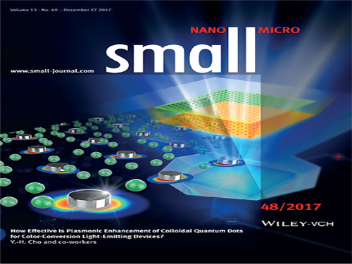 Realizing Highly Efficient Quantum Dot LEDs with Metallic Nanostructures
(Professor Yong-Hoon Cho and PhD candidate Hyun Chul Park)
KAIST researchers have discovered a technology that enhances the efficiency of Quantum Dot LEDs.
Professor Yong-Hoon Cho from the Department of Physics and his team succeeded in improving the efficiency of Quantum Dot (QD) Light-Emitting Diodes (LEDs) by designing metallic nanostructure substrates.
QD LEDs possess very small semiconductor light sources and are considered to be the new rising technology for high performance full-color display. However, it is expensive to manufacture displays with QD LED only.
Existing QD-based displays use blue LEDs as a source of light, and they employ a method of color conversion through excitation of green and red QDs.
There are two inconveniences with the existing QD-based displays. As mentioned previously, QD LED is costly, hence the unit price of QD-based displays is higher. Also, the efficiency of a liquid type of QDs is drastically lowered after contact with air.
Professor Cho found the solution in a metallic nanostructure for lowering the production cost while improving the efficiency of QD LEDs.
The team exploited the phenomenon of so-called surface plasmonic resonances when nanoscale metallic structures are exposed to light. Depending on the metal, the size, and the shape, the properties of metallic structures vary.
The team used different metallic nanostructures for each QD LED – silver nanodisks for Red QDs and aluminum nanodisks for Green GDs – to make them more fluorescent.
With brighter QDs, it requires fewer QDs to manufacture QD LEDs, contributing to a lower unit price.
The team used silver and aluminum in this research, but metallic nanostructures can be redesigned according to the desired purposes.
Professor Cho said, “Implementing metallic nanostructures into QD LEDs in a proper manner can reduce the quantity of the QDs required for the system, leading to lower unit prices.”
This research, led by PhD candidate Hyun Chul Park, was chosen as the cover of the international journal, Small, on December 27, 2017.
Figure 1. Cover of the journal
Figure 2. Spectrum showing different fluorescence with and without metallic nanostructure
2018.01.23 View 6068
Realizing Highly Efficient Quantum Dot LEDs with Metallic Nanostructures
(Professor Yong-Hoon Cho and PhD candidate Hyun Chul Park)
KAIST researchers have discovered a technology that enhances the efficiency of Quantum Dot LEDs.
Professor Yong-Hoon Cho from the Department of Physics and his team succeeded in improving the efficiency of Quantum Dot (QD) Light-Emitting Diodes (LEDs) by designing metallic nanostructure substrates.
QD LEDs possess very small semiconductor light sources and are considered to be the new rising technology for high performance full-color display. However, it is expensive to manufacture displays with QD LED only.
Existing QD-based displays use blue LEDs as a source of light, and they employ a method of color conversion through excitation of green and red QDs.
There are two inconveniences with the existing QD-based displays. As mentioned previously, QD LED is costly, hence the unit price of QD-based displays is higher. Also, the efficiency of a liquid type of QDs is drastically lowered after contact with air.
Professor Cho found the solution in a metallic nanostructure for lowering the production cost while improving the efficiency of QD LEDs.
The team exploited the phenomenon of so-called surface plasmonic resonances when nanoscale metallic structures are exposed to light. Depending on the metal, the size, and the shape, the properties of metallic structures vary.
The team used different metallic nanostructures for each QD LED – silver nanodisks for Red QDs and aluminum nanodisks for Green GDs – to make them more fluorescent.
With brighter QDs, it requires fewer QDs to manufacture QD LEDs, contributing to a lower unit price.
The team used silver and aluminum in this research, but metallic nanostructures can be redesigned according to the desired purposes.
Professor Cho said, “Implementing metallic nanostructures into QD LEDs in a proper manner can reduce the quantity of the QDs required for the system, leading to lower unit prices.”
This research, led by PhD candidate Hyun Chul Park, was chosen as the cover of the international journal, Small, on December 27, 2017.
Figure 1. Cover of the journal
Figure 2. Spectrum showing different fluorescence with and without metallic nanostructure
2018.01.23 View 6068 -
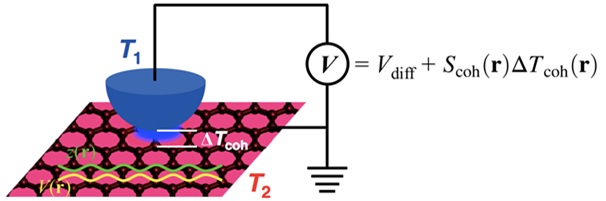 An Electron Cloud Distribution Observed by the Scanning Seebeck Microscope
All matters are made of small particles, namely atoms. An atom is composed of a heavy nucleus and cloud-like, extremely light electrons.
Korean researchers developed an electron microscopy technique that enables the accurate observation of an electron cloud distribution at room-temperature. The achievement is comparable to the invention of the quantum tunneling microscopy technique developed 33 years ago.
Professor Yong-Hyun Kim of the Graduate School of Nanoscience and Technology at KAIST and Dr. Ho-Gi Yeo of the Korea Research Institute of Standards and Science (KRISS) developed the Scanning Seebeck Microscope (SSM). The SSM renders clear images of atoms, as well as an electron cloud distribution. This was achieved by creating a voltage difference via a temperature gradient.
The development was introduced in the online edition of Physical Review Letters (April 2014), a prestigious journal published by the American Institute of Physics.
The SSM is expected to be economically competitive as it gives high resolution images at an atomic scale even for graphene and semiconductors, both at room temperature. In addition, if the SSM is applied to thermoelectric material research, it will contribute to the development of high-efficiency thermoelectric materials.
Through numerous hypotheses and experiments, scientists now believe that there exists an electron cloud surrounding a nucleus. IBM's Scanning Tunneling Microscope (STM) was the first to observe the electron cloud and has remained as the only technique to this day. The developers of IBM microscope, Dr. Gerd Binnig and Dr. Heinrich Rohrer, were awarded the 1986 Nobel Prize in Physics.
There still remains a downside to the STM technique, however: it required high precision and extreme low temperature and vibration. The application of voltage also affects the electron cloud, resulting in a distorted image.
The KAIST research team adopted a different approach by using the Seebeck effect which refers to the voltage generation due to a temperature gradient between two materials.
The team placed an observation sample (graphene) at room temperature (37~57℃) and detected its voltage generation. This technique made it possible to observe an electron cloud at room temperature.
Furthermore, the research team investigated the theoretical quantum mechanics behind the electron cloud using the observation gained through the Seebeck effect and also obtained by simulation capability to analyze the experimental results.
The research was a joint research project between KAIST Professor Yong-Hyun Kim and KRISS researcher Dr. Ho-Gi Yeo. Eui-Seop Lee, a Ph.D. candidate of KAIST, and KRISS researcher Dr. Sang-Hui Cho also participated. The Ministry of Science, ICT, and Future Planning, the Global Frontier Initiative, and the Disruptive Convergent Technology Development Initiative funded the project in Korea.
Picture 1: Schematic Diagram of the Scanning Seebeck Microscope (SSM)
Picture 2: Electron cloud distribution observed by SSM at room temperature
Picture 3: Professor Yong-Hyun Kim
2014.04.04 View 10959
An Electron Cloud Distribution Observed by the Scanning Seebeck Microscope
All matters are made of small particles, namely atoms. An atom is composed of a heavy nucleus and cloud-like, extremely light electrons.
Korean researchers developed an electron microscopy technique that enables the accurate observation of an electron cloud distribution at room-temperature. The achievement is comparable to the invention of the quantum tunneling microscopy technique developed 33 years ago.
Professor Yong-Hyun Kim of the Graduate School of Nanoscience and Technology at KAIST and Dr. Ho-Gi Yeo of the Korea Research Institute of Standards and Science (KRISS) developed the Scanning Seebeck Microscope (SSM). The SSM renders clear images of atoms, as well as an electron cloud distribution. This was achieved by creating a voltage difference via a temperature gradient.
The development was introduced in the online edition of Physical Review Letters (April 2014), a prestigious journal published by the American Institute of Physics.
The SSM is expected to be economically competitive as it gives high resolution images at an atomic scale even for graphene and semiconductors, both at room temperature. In addition, if the SSM is applied to thermoelectric material research, it will contribute to the development of high-efficiency thermoelectric materials.
Through numerous hypotheses and experiments, scientists now believe that there exists an electron cloud surrounding a nucleus. IBM's Scanning Tunneling Microscope (STM) was the first to observe the electron cloud and has remained as the only technique to this day. The developers of IBM microscope, Dr. Gerd Binnig and Dr. Heinrich Rohrer, were awarded the 1986 Nobel Prize in Physics.
There still remains a downside to the STM technique, however: it required high precision and extreme low temperature and vibration. The application of voltage also affects the electron cloud, resulting in a distorted image.
The KAIST research team adopted a different approach by using the Seebeck effect which refers to the voltage generation due to a temperature gradient between two materials.
The team placed an observation sample (graphene) at room temperature (37~57℃) and detected its voltage generation. This technique made it possible to observe an electron cloud at room temperature.
Furthermore, the research team investigated the theoretical quantum mechanics behind the electron cloud using the observation gained through the Seebeck effect and also obtained by simulation capability to analyze the experimental results.
The research was a joint research project between KAIST Professor Yong-Hyun Kim and KRISS researcher Dr. Ho-Gi Yeo. Eui-Seop Lee, a Ph.D. candidate of KAIST, and KRISS researcher Dr. Sang-Hui Cho also participated. The Ministry of Science, ICT, and Future Planning, the Global Frontier Initiative, and the Disruptive Convergent Technology Development Initiative funded the project in Korea.
Picture 1: Schematic Diagram of the Scanning Seebeck Microscope (SSM)
Picture 2: Electron cloud distribution observed by SSM at room temperature
Picture 3: Professor Yong-Hyun Kim
2014.04.04 View 10959